Toshiba and Japan Semiconductor develop auto analogue process
The 0.13-micron process applied to analogue ICs is claimed to offer an optimized combination of processes and devices, according to rated voltage, performance, reliability and cost, for automotive analogue circuits and eNVM on a single chip.
Analogue ICs, including motor driver ICs, are used in a wide range of automotive applications. With the transition to electric vehicles and increase of vehicles with ADAS, the analogue IC market is expected to see continuous growth.
This has created a requirement for a versatile, dedicated automotive platform that can meet a wide range of requirements related to automotive applications.
As eNVM and a microcontroller unit (MCU) have not been realized on a single chip, the total IC area is large.
Toshiba and Japan Semiconductor offer three LDMOS structures and a very wide device lineup, including eNVM, that are selectable to meet diverse requirements.
Now they have developed what is claimed to be a highly reliable process for analogue ICs that meets AEC-Q100/Grade-0, an international standard in automotive reliability.
There has been a trade-off between on-resistance (RonA), a key parameter for LDMOS, and breakdown voltage between drain and source (BVDSS).
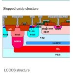
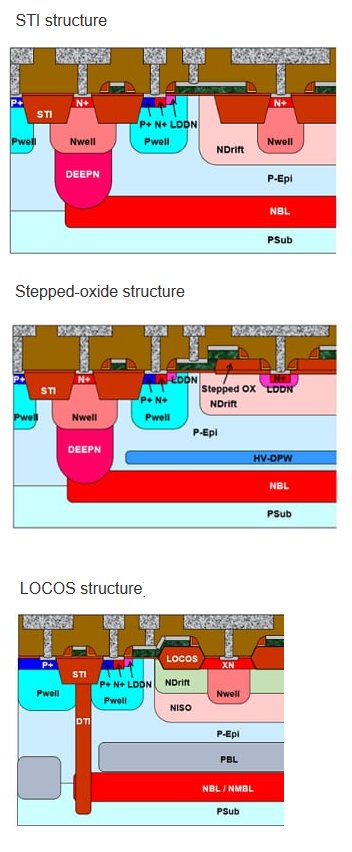
The lower the RonA, the better the performance with a constant BVDSS. Toshiba and Japan Semiconductor confirmed that two kinds of LDMOS, with stepped-oxide or LOCOS located between the drain and source, have a maximum RonA that is 44%*3 better than STI-based LDMOS.
They also determined mechanisms to evaluate the advantages of LOCOS-based LDMOS’s device reliability, failure rates and ESD tolerance.
eNVM from Floadia Corporation (Floadia LEE Flash G1) embedded in the platform is provided with only three additional masks.
They can satisfy high-reliability requirements for automotive analog power devices without impacting on base platforms and devices.
They also avoid mal-function in the eNVM by optimizing layout to protect it from the noise caused by switching LDMOS in the analogue circuits.
Toshiba and Japan Semiconductor plan to start sampling automotive semiconductors with the newly developed platform in December 2022.
LDMOS: Lateral Double Diffused MOS (Metal Oxide Semiconductor).
LOCOS: LOCal Oxidation of Silicon. Utilize Silicon nitride film as a hard mask and selectively create a Silicon oxide film on Si substrate, and isolates elements.
Toshiba and Japan Semiconductor confirmed that two kinds of LDMOS, with stepped-oxide or LOCOS located between the drain and source, have a maximum RonA that is 44% better than STI-based LDMOS, Toshiba test results.
STI: Shallow Trench Isolation. Isolates elements by embedding insulator film into shallow trenches.
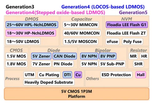
Device line-up of the developed platform
Structures of the three kinds of LDMOS structure
Floadia’s eNVM TEM image and the evaluation result of endurance test and data retention test (Toshiba test results)
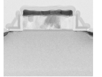
(a) eNVM TEM Image
(b) endurance test
(c) data retention test